Advanced Node Wafer Defect Inspection Systems Market to Reach USD 8.87 Billion by 2036 as Sub-5nm Complexity Drives Full-Wafer Scanning Adoption
 Rising at an 11.30% CAGR, the market is fueled by gate-all-around architectures, EUV process challenges, and the shift from sampling to exhaustive inline inspection
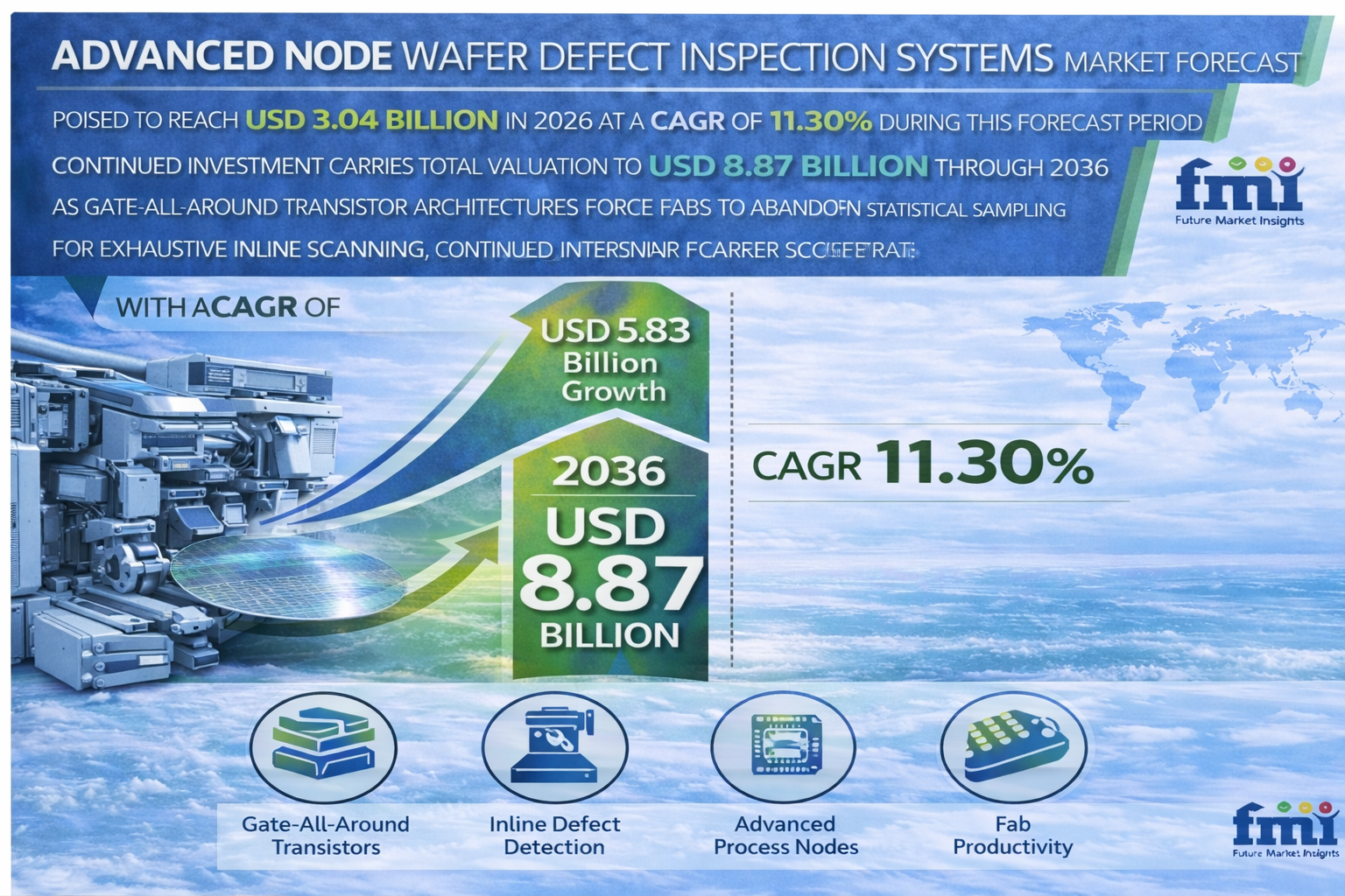
NEWARK, DE / ACCESS Newswire / March 24, 2026 / The global advanced node wafer defect inspection systems market is entering a precision-driven growth phase as semiconductor manufacturers accelerate investments in next-generation inspection technologies to support sub-5nm and angstrom-era production. Valued at USD 2.73 billion in 2025, the market is projected to reach USD 3.04 billion in 2026 and further expand to USD 8.87 billion by 2036, registering a CAGR of 11.30% during the forecast period.
This growth reflects a structural transformation in semiconductor manufacturing, where traditional statistical sampling methods are becoming obsolete. With the adoption of gate-all-around (GAA) transistor architectures and extreme ultraviolet (EUV) lithography, fabs are increasingly shifting toward exhaustive inline scanning to detect nanoscale defects that can compromise entire production batches.
Get Access of Report Sample:
https://www.futuremarketinsights.com/reports/sample/rep-gb-32450
Market Value Analysis: Yield Learning Pressures Accelerating Capital Investment
Between 2026 and 2030, the advanced node wafer defect inspection systems market is expected to witness strong capital inflows as leading-edge fabs prioritize yield optimization at 3nm and below. Process integration teams face a critical trade-off: relying on high-speed optical inspection for throughput or deploying slower e-beam systems for deep defect visibility.
Semiconductor manufacturers are increasingly prioritizing:
High-throughput optical inspection systems for inline screening
Dense e-beam scanning platforms for sub-surface defect detection
AI-driven defect classification software to reduce false positives
Integrated inspection clusters within production lines
Delaying investment in advanced inspection tools exposes fabs to undetected defect propagation, leading to significant yield losses and financial risk.
From 2030 to 2036, growth will be driven by seamless integration of inspection hardware with advanced software ecosystems, enabling faster qualification cycles and real-time process control.
Technology Evolution: AI-Driven Classification and Hybrid Inspection Architectures
The evolution of wafer defect inspection systems is being shaped by the convergence of advanced optics, electron-beam technology, and machine learning algorithms. Key innovations include:
High-speed optical brightfield and darkfield inspection systems
Multi-beam e-beam platforms for nanoscale defect detection
AI-powered classification engines to distinguish nuisance vs. killer defects
Real-time data processing for inline yield monitoring
Hybrid inspection workflows combining optical and e-beam capabilities
A major breakthrough lies in automated defect classification. Once machine learning algorithms can accurately filter out non-critical defects without human intervention, fabs achieve exponential gains in throughput and yield learning efficiency.
An industry analyst notes:
"Inspection accuracy is no longer defined by resolution alone-it is determined by how effectively systems classify and prioritize defects. Without intelligent filtering, even the most advanced scanners create operational bottlenecks."
Precision Metrology Becoming Central to Semiconductor Manufacturing
As semiconductor nodes shrink below 5nm, defect inspection systems are evolving into mission-critical infrastructure within fabrication facilities. These systems enable:
Detection of sub-surface voids and micro-bridges in GAA structures
Continuous monitoring of patterned wafers across multiple process steps
Real-time process control to prevent yield excursions
Optimization of EUV lithography performance
Reduction of downstream packaging failures
This shift is redefining competitive dynamics in the semiconductor industry, where yield performance directly impacts profitability and market leadership.
Segment Spotlight
Optical Inspection Leads Technology Segment (48.0%)
Optical systems dominate due to unmatched throughput, enabling rapid full-wafer scanning during high-volume production.
Patterned Wafer Inspection Leads Mode Segment (57.0%)
Complex multi-layer patterning requires continuous monitoring to detect cumulative defects.
3nm Node Leads Node Segment (39.0%)
Current volume production at 3nm drives demand for advanced inspection tools.
Foundries Lead End-Use Segment (46.0%)
Pure-play foundries account for the majority of capital expenditure in advanced inspection systems.
Inline Monitoring Leads Workflow Stage (44.0%)
Real-time inspection enables immediate detection and correction of process deviations.
Regional Insights: Asia-Pacific Dominates Advanced Node Inspection Investments
Country
CAGR (2026-2036)
Key Growth Drivers
Taiwan
12.6%
Aggressive N2 node investments and yield-learning initiatives
South Korea
11.8%
Foundry expansion and advanced memory integration
United States
10.9%
Domestic capacity expansion and advanced node development
Japan
10.4%
Strong material science and precision engineering capabilities
Singapore
9.6%
Regional hub for advanced semiconductor manufacturing
Germany
8.8%
Focus on high-reliability automotive semiconductor production
China
8.1%
Localized innovation despite export constraints
Opportunities: AI, Backside Inspection, and Clustered Architectures Unlock Growth
Key growth opportunities in the market include:
Advanced machine learning algorithms for defect classification
Backside power delivery inspection systems for next-generation architectures
Clustered inspection platforms integrated with process equipment
Edge computing solutions for real-time data processing
High-throughput hybrid inspection systems
These innovations are enabling faster yield ramp cycles, reduced operational costs, and improved manufacturing efficiency.
Competitive Landscape: Few Players Dominate High-Barrier Market
The advanced node wafer defect inspection systems market is characterized by extremely high entry barriers, with a limited number of global players dominating the space.
Leading companies include:
KLA Corporation
ASML Holding N.V.
Applied Materials, Inc.
Hitachi High-Tech Corporation
Onto Innovation Inc.
Lasertec Corporation
SCREEN Semiconductor Solutions Co., Ltd.
Competitive differentiation is increasingly driven by:
Integration of hardware and AI-driven software platforms
Ability to deliver hybrid inspection solutions
Proprietary defect data libraries for machine learning
Seamless integration with fab production environments
Future Outlook: Inspection Systems Becoming the Backbone of Advanced Semiconductor Manufacturing
Looking ahead to 2036, advanced node wafer defect inspection systems will become foundational to semiconductor fabrication as nodes continue to shrink and process complexity intensifies.
Key trends shaping the market include:
Transition to exhaustive full-wafer inspection at all critical layers
Expansion of AI-driven defect classification systems
Integration of inspection tools within clustered manufacturing environments
Rising importance of data analytics in yield optimization
Growth of angstrom-era semiconductor manufacturing
As the semiconductor industry advances toward increasingly complex architectures, defect inspection systems will play a decisive role in determining yield success, operational efficiency, and long-term competitiveness.
For an in-depth analysis of evolving formulation trends and to access the complete strategic outlook for the Advanced Node Wafer Defect Inspection Systems Market through 2036, visit the official report page at: https://www.futuremarketinsights.com/reports/advanced-node-wafer-defect-inspection-systems-market
Browse More Technology Industry Reports:
Event Management Software Market - https://www.futuremarketinsights.com/reports/event-management-software-market
Crystal Oscillator Market - https://www.futuremarketinsights.com/reports/crystal-oscillator-market
Visitor Management System Market - https://www.futuremarketinsights.com/reports/visitor-management-system-market
Fleet Management Market - https://www.futuremarketinsights.com/reports/fleet-management-market
Security Screening Market - https://www.futuremarketinsights.com/reports/security-screening-market
About Future Market Insights (FMI)
Future Market Insights (FMI) is a leading provider of market intelligence and consulting services, serving clients in over 150 countries. Headquartered in Delaware, USA, with a global delivery center in India and offices in the UK and UAE, FMI delivers actionable insights to businesses across industries including automotive, technology, consumer products, manufacturing, energy, and chemicals.
An ESOMAR-certified research organization, FMI provides custom and syndicated market reports and consulting services, supporting both Fortune 1,000 companies and SMEs. Its team of 300+ experienced analysts ensures credible, data-driven insights to help clients navigate global markets and identify growth opportunities.
For Press & Corporate Inquiries
Rahul Singh
AVP - Marketing and Growth Strategy
Future Market Insights, Inc.
+91 8600020075
For Sales - [email protected]
For Media - [email protected]
For web - https://www.futuremarketinsights.com/
SOURCE: Future Market Insights, Inc.